💡 Researchers optimize backside ohmic contacts for N-face GaN, unlocking the potential of fully vertical GaN-on-Silicon power devices.
⚡️ Gallium Nitride (GaN) has been making waves in the power electronics world, promising to outperform traditional silicon-based devices. But there's been a catch – the tricky business of creating efficient backside contacts in fully vertical GaN-on-Silicon structures. Well, folks, it looks like we've got a breakthrough on our hands! 🎉
A team of researchers from various institutions, including CNRS-IEMN and Ghent University, have cracked the code on optimizing non-alloyed ohmic contacts on the N-polar n+-doped GaN face backside layer. This might sound like a mouthful, but trust me, it's a game-changer for the future of power devices.
So, what's the big deal? 🤔 These fully vertical GaN structures could lead to more compact and efficient power devices, potentially revolutionizing everything from our smartphone chargers to electric vehicle powertrains. The key was finding a way to create low-resistance ohmic contacts on the nitrogen face of the n+ layer – a task that's been giving engineers headaches for years.
The secret sauce? A simple HCl treatment! 🧪 By applying hydrochloric acid at 70°C for just 3 minutes, the team managed to significantly reduce the specific contact resistance without any additional annealing. This means the process is fully compatible with frontside processing, making it a practical solution for real-world manufacturing.
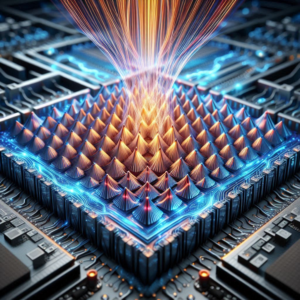
But wait, there's more! 🔬 The researchers didn't just stumble upon this solution – they meticulously investigated the impact of treatment time and temperature, and even dove into the nitty-gritty of surface chemistry using XPS and SEM analysis. They found that the HCl treatment not only removes pesky surface oxides but also creates tiny pyramid structures that play a crucial role in the contact's performance.
The best part? This technique isn't just effective – it's also thermally stable up to 300°C, making it robust enough for real-world applications. 💪
As we continue to push the boundaries of power electronics, innovations like this are crucial for developing the next generation of energy-efficient devices. So, the next time you plug in your phone or hop into an electric car, remember – there might be a little bit of HCl-treated GaN magic making it all possible!
Source: Hamdaoui, Y.; Vandenbroucke, S.S.T.; Michler, S.; Ziouche, K.; Minjauw, M.M.; Detavernier, C.; Medjdoub, F. Optimization of Non-Alloyed Backside Ohmic Contacts to N-Face GaN for Fully Vertical GaN-on-Silicon-Based Power Devices. Micromachines 2024, 15, 1157. https://doi.org/10.3390/mi15091157